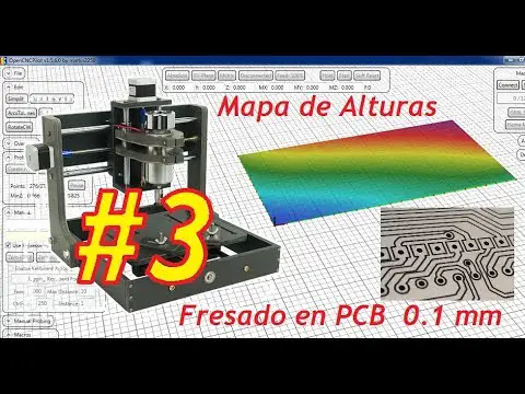
Effective Techniques for Milling PCBs at Home
Welcome to my new article! Today I will talk to you about one of my great passions: electronics. If you are a fan of this discipline, you surely know that the manufacture of printed circuit boards (PCB) is one of the most important tasks in the creation of any electronic device. However, it is not always easy to do it at home. Therefore, on this occasion I bring you some effective techniques for milling PCBs at home, so that you can enjoy the satisfaction of creating your own boards from the comfort of your home. Get ready to learn and have fun!
Become an expert in PCB manufacturing with these milling techniques
Become an expert in PCB manufacturing with these milling techniques
PCB (Printed Circuit Board) manufacturing is a crucial process for any electronics project. Although they can be ordered from specialized companies, doing it at home can be a cheaper and more convenient option. Here are some effective techniques for milling PCBs at home:
- Preparation: Before you start, make sure you have all the necessary tools, such as a CNC router, copper plate, carbide drill bit, photo mask, and ferric acid. It is also important to have a clear and precise design of the PCB that you want to manufacture.
- Creating the photo mask: The photographic mask is a sheet that adheres to the copper plate and protects the areas that you do not want to engrave. The design must be printed on transparent paper, placed on the mask and exposed to a UV light so that it adheres to the plate. The sheet is then removed and developed with water to reveal the areas to be engraved.
- milling: Once the photo mask is in place, the copper plate is placed on the CNC router and the carbide bit is fitted. The design is programmed into the milling machine and milling begins. It is important to do it carefully and in several passes to avoid damaging the plate.
- Remove the mask: After reaming the plate, the photographic mask should be removed with a ferric acid solution. Immerse the plate in the acid and shake gently until the entire plate is removed. It is then washed with water to remove any acid residue and allowed to dry.
- Drilling: Finally, the necessary holes for the components must be made on the PCB. A smaller diameter drill bit than the milling one is used and the holes are made in the places indicated in the design.
In short, milling PCBs at home requires a careful and precise process, but it can be an economical and useful alternative for any electronics project. With the right techniques and the necessary tools, anyone can become an expert in PCB manufacturing. Dare to try it!
Comparison of PCB design programs: Find the right one for you
Comparison of PCB design programs: Find the right one for you
If you are looking for a program for PCB (printed circuit board) design, you will likely find a large number of options available. Each program has its own features and benefits, so it is important to select the right one for your needs. Here we present a comparison of some of the most popular programs for designing PCBs.
1. Altium Designer
Altium Designer is a PCB design program with a friendly and easy-to-use interface. It is a popular choice among engineers and designers due to its wide range of tools and features. The program also offers a large number of component libraries, making the design process even easier.
2.Eagle PCB
Eagle PCB is one of the most popular software for PCB designing. It is easy to use and offers a large number of tools and component libraries. Eagle PCB is especially useful if you are looking for a cost-effective solution for PCB design.
3. KiCad
KiCad is an open source PCB design program with an active community of users. It offers a wide range of tools and functions for PCB design, as well as a large number of component libraries. KiCad is also compatible with a variety of platforms, making it a popular choice among Mac and Linux users.
4. Proteus
Proteus is a PCB design program with an easy-to-use interface and a wide range of tools and features. It offers built-in circuit simulation, allowing you to test your design before building it. Proteus also has a large number of component libraries, making the design process even easier.
5.DipTrace
DipTrace is a PCB design program with an intuitive and easy-to-use interface. It offers a wide range of tools and functions, as well as a large number of component libraries. DipTrace also has a free version available, making it a popular option for those on a budget.
6. EasyEDA
EasyEDA is an online PCB design program that offers a friendly and easy-to-use interface. It offers a wealth of tools and features, as well as an ever-growing library of components. EasyEDA also allows you to share your designs with other users, making it a popular choice among collaborative designers.
Conclusion
In short, there are a large number of programs available for PCB design. It is important to select the right one for your specific needs. If you're looking for an easy-to-use and affordable option, Eagle PCB and DipTrace are great options. If you need a wide range of tools and features, Altium Designer and Proteus are great options. And if you're looking for an open source option with an active community of users, KiCad is a great option.
Optimize your PCB ironing time with these tips
Optimize your PCB ironing time with these tips
Ironing a PCB is an essential task in electronic circuit manufacturing. Here are some tips to optimize your ironing time and achieve successful results.
- Organize your workspace: Before you start, make sure you have everything you need on hand. This includes the printed circuit board, transfer paper, iron, sandpaper, and paper remover.
- Prepare the board: Gently sand the printed circuit board to make the surface smooth.
This will ensure better transfer of the design. - Printing the design: print the design on the transfer paper with the laser printer. Make sure the design is in the correct position and that the transfer paper is well aligned with the printed circuit board.
- Ironing: Place the transfer paper with the design on the printed circuit board and use the hot iron to transfer the design to the board. Make sure you apply enough pressure and heat for a complete and even transfer.
- Removing the transfer paper: After ironing the plate, dip the plate in hot water to soften the transfer paper. Then, use the paper remover to completely remove the transfer paper.
- Drilling: Use a carbide drill bit to drill holes in the printed circuit board. Make sure the holes are in the correct position and are large enough for the components that will be used.
- Clean the plate: Use a plate cleaner to remove any transfer paper or perforation residue.
By following these tips, you will be able to optimize your ironing time and achieve successful results in the manufacture of electronic circuits.
Know the right drill bit for creating PCBs in electronics
Know the right drill bit for creating PCBs in electronics
To create a printed circuit board (PCB) at home, it is important to choose the right drill bit to achieve an effective and precise result. Here we present the most effective techniques for milling PCBs at home:
- Carbide drill bits: They are best suited for milling PCBs as they have a long lifespan and are very resistant to the heat generated by the friction of the bit with the board. In addition, they are very precise and can create very small diameter holes.
- Tungsten drill bits: They are an alternative to carbide bits, but have a shorter lifespan and are not as heat resistant. However, they are cheaper and can be a good option for those who don't make PCBs often.
- Diamond drill bits: They are the most accurate and durable, but they are also the most expensive. They are mainly used in the electronics industry to create high-quality PCBs.
It is important to note that to mill PCBs at home, you need to have a high-speed drill and a board holder. In addition, it is recommended to use a PCB milling cutter, which is a tool specially designed for creating printed circuits.
To choose the right drill bit, it is important to consider the size of the holes and the precision required in the circuit design. Below is a table with the most common drill bit sizes for creating PCBs:
| drill bit size | Hole diameter |
|---|---|
| 0.6 mm | 0.8 mm |
| 0.8 mm | 1.0 mm |
| 1.0 mm | 1.2 mm |
| 1.2 mm | 1.4 mm |
| 1.4 mm | 1.6 mm |
In short, choosing the right drill bit is essential for creating precise and effective PCBs. Carbide drill bits are the most recommended for milling PCBs at home, but it is important to evaluate each person's needs and budget to choose the best option. In addition, it is important to take into account the size of the holes and use specialized tools to achieve an optimal result.
How to Make Your Own PCBs with Homemade Screen Printing: A Complete Guide for Electronics Hobbyists.
To make your own PCBs with homemade screen printing, you can follow the following steps:
1. Design your PCB in circuit design software such as Eagle or KiCAD. Make sure the design is clear and easy to follow.
2. Print your design on transparent paper with a laser printer. Make sure the print is high quality and the image is inverted.
3. Place the printed sheet with the design on the copper plate and secure it with adhesive tape.
4. Prepare a ferric chloride solution and immerse the copper plate with the printed sheet facing down. Shake the plate gently to ensure that the ferric chloride covers the entire surface.
5. After a few minutes, remove the plate from the ferric chloride and rinse it with water. Remove the printed sheet and clean the plate with a soft brush and water.
6. Now, you need to do the screen printing on the plate. To do this, you can use a permanent marker or special screen printing transfer paper.
7. Once the silkscreen is dry, place the board on a CNC drill and router to remove excess copper and create the circuit paths.
8. Finally, clean the board with isopropyl alcohol and verify that the circuit works correctly.
In summary, the steps to make your own PCBs with homemade screen printing are:
- Design your PCB in circuit design software
- Print your design on transparent paper with a laser printer
- Place the printed sheet with the design on the copper plate and immerse the plate in a ferric chloride solution
- Clean the plate and do the screen printing on the plate
- Route the board to remove excess copper and create the circuit paths
- Clean the board with isopropyl alcohol and verify that the circuit works correctly
With these effective techniques for milling PCBs at home, you can make your own printed circuit boards efficiently and economically.
You already have it! With these effective techniques for milling PCBs at home, you will be able to create your own printed circuits with ease and precision. Let's get to work and create your own electronic projects!


Post Comment